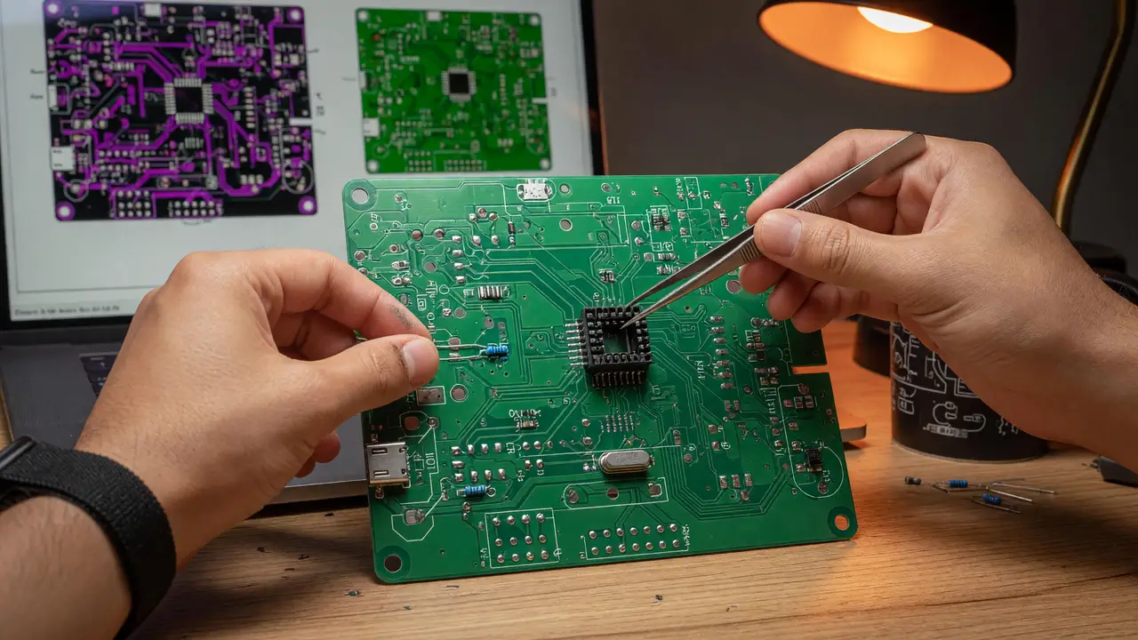
How to Design Your First Custom Printed Circuit Board (PCB) in KiCad
Step-by-step guide to designing your first custom PCB in KiCad 10, from schematic capture and layout to DRC, 3D preview, and ordering boards from JLCPCB or OSH Park.
Not long ago, spinning a custom PCB meant either paying for pricey software or grinding through a brutal learning curve. KiCad 10 removes most of that friction. The open-source suite, now at stable version 10.0.4, gives you a complete path from schematic to fabrication files, plus a solid 3D viewer and noticeably better routing tools.
Getting Started with KiCad 10
Grab the latest build from kicad.org. It runs fine on 64-bit machines with 1 GB of RAM (8 GB feels more comfortable), OpenGL 2.1 or newer graphics, and about 10 GB of free space. Windows 10/11, macOS 13 and up, and current Linux distros are all supported.
Installation is quick. Open the project manager, pick a folder, and name your project. The launcher now keeps the main tools—schematic editor, PCB editor, and 3D viewer—within easy reach instead of burying them in menus.
Building the Schematic
Open the schematic editor and drop in parts from the built-in libraries or any footprints you’ve downloaded. Wire the components together, give everything sensible reference designators, then use the Assign Footprints tool to match each symbol to a real package.
A simple LED blink circuit with an ATtiny85 makes a good first project. Keep the drawing readable: label your nets, add power flags, and run the electrical rules checker (ERC) early so you catch problems before they reach the layout stage.
Moving to PCB Layout and 3D Preview
Switch to the PCB editor and pull the netlist across with “Update PCB from Schematic.” Place the parts, draw the board outline on the Edge.Cuts layer, and start routing. The improved push-and-shove router and length-tuning features make this step faster than it used to be.
Once the traces are done, open the 3D viewer (View → 3D Viewer). Spin the board around, check clearances, and make sure nothing sticks up too high. Mechanical issues that would only show up after ordering become obvious here.
Design Checks, Export, and Ordering
Run the design rule checker (DRC) using your board house’s limits—most cheap prototype services handle 6 mil traces and 6 mil spacing without trouble. Fix any violations, then generate the Gerbers along with drill files and pick-and-place data.
2026 Fabrication Pricing (2-Layer, 100×100 mm)
| Vendor | Boards | Base Price | Landed Cost (US, incl. tariffs) | Notes |
|---|---|---|---|---|
| JLCPCB | 5 | $2 | $25–35 | Best for larger boards |
| PCBWay | 5 | $5 | $28–38 | Good assembly options |
| OSH Park | 3 | ~$77.50 | $77.50 | US-made, no duties |
Small boards often cost less at OSH Park; bigger ones still come out ahead from the Asian fabs once tariffs are factored in.
Practical Workflow Summary
flowchart LR
    A[Create Schematic] --> B[Assign Footprints]
    B --> C[PCB Layout & Routing]
    C --> D[DRC + 3D Check]
    D --> E[Export Gerbers]
    E --> F[Order Boards]
Stick to that order on every project. Save versions as you go and keep your libraries tidy.
Conclusion
KiCad 10 gives you a reliable, zero-cost route from idea to assembled board. Begin with something small, get comfortable moving from schematic to layout, and lean on the 3D viewer and DRC tools to avoid expensive surprises. Check current fab pricing before you order—OSH Park for quick domestic runs, JLCPCB or PCBWay when you want to keep costs down. Your second board will already feel easier than the first.