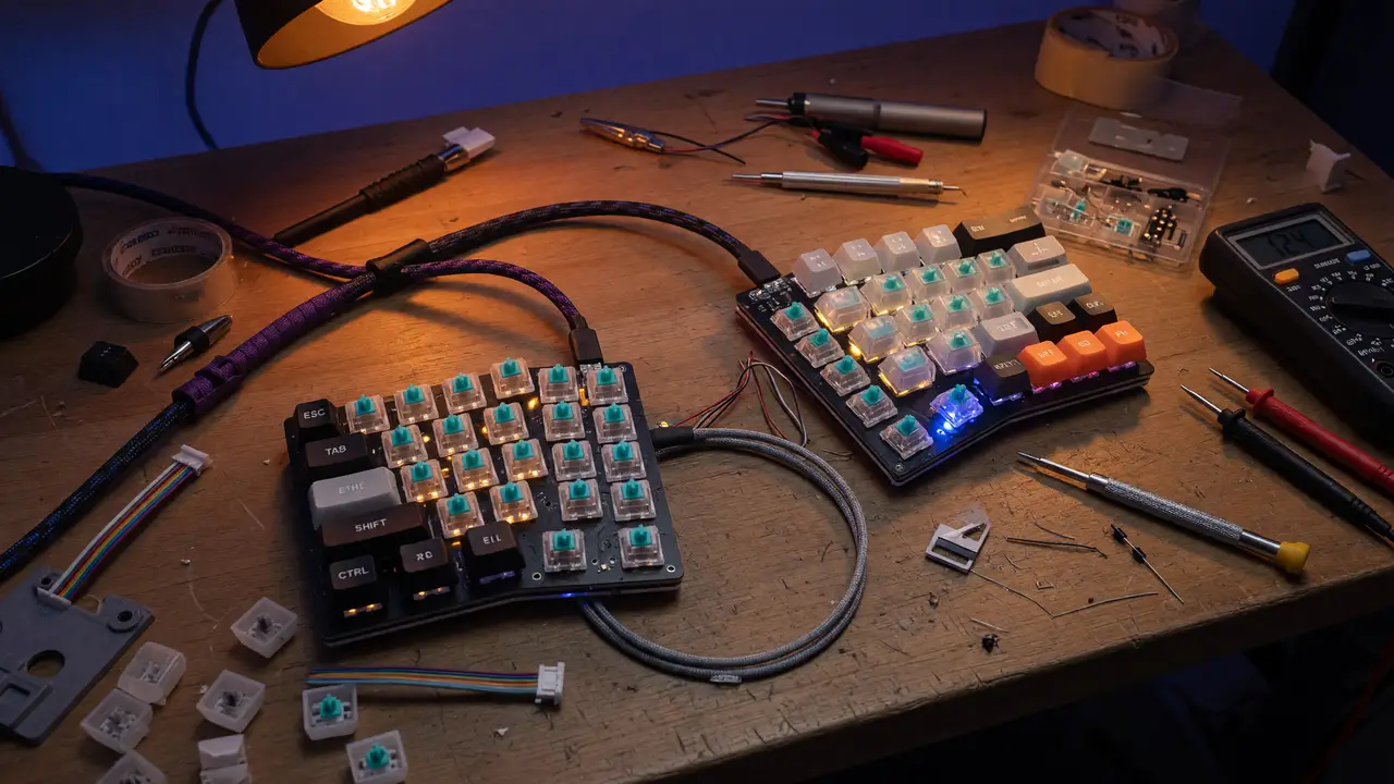
Mechanical Keyboard Prototyping: Designing a Custom Split Layout in Ergogen
Learn how to prototype custom split mechanical keyboards using Ergogen. Turn a single YAML file into KiCad PCBs, cases, and outlines in minutes.
Custom split keyboards feel far more comfortable than most ready-made options, yet many builders still spend days fiddling with layouts and PCB work. Ergogen speeds things up by turning one YAML file into outlines, cases, and unrouted KiCad boards.
The process goes from config to fabrication files in minutes.
Why Ergogen for Split Layouts
Ergogen v4.0.0 supports reversible halves, column-staggered matrices, and ZMK-ready outputs directly from YAML. It spits out DXF/SVG outlines, JSCAD cases, and KiCad PCB skeletons so you skip the manual coordinate math.
Take layouts like Porcupine (36–42 keys) or various Corne clones. They show the tool in action. Common stagger values put the ring finger column at 5 mm, middle at 2.5 mm, and index at –2.5 mm from the one before. Drop those straight into Ergogen’s stagger keys.
Core YAML Structure
A basic split begins with units, points, and outlines. This 36-key column-staggered half gives you the idea:
points:
  zones:
    matrix:
      columns:
        pinky:
          stagger: 5
        ring:
          stagger: 2.5
        middle:
          stagger: -2.5
      rows:
        bottom:
          bind: 5
  key:
    footprints:
      choc: true
Run ergogen config.yaml and the CLI hands back the layout plus raw points for checking. You can load external footprints through the web UI at ergogen.xyz without trouble.
Output Formats and Workflow
Ergogen produces four main files:
- DXF/SVG outlines for plates
- JSCAD cases (convert to STL when needed)
- Unrouted
kicad_pcbfiles with switches and diodes placed - YAML exports for further scripting
A typical flow looks like this:
flowchart TD
    A[YAML config] --> B[Ergogen CLI]
    B --> C[DXF/SVG outlines]
    B --> D[JSCAD case]
    B --> E[KiCad PCB skeleton]
    E --> F[Manual routing in KiCad]
    F --> G[JLCPCB order]
Reversible patterns and Nice!Nano cutouts now sit in the official guides. Matrix routing stays manual—Ergogen places the footprints but leaves the traces to you.
Prototype Cost Breakdown
Most complete wired or wireless splits built between 2023 and 2025 land between $99 and $200. The table below shows typical JLCPCB pricing and component counts for a 36-key design.
| Item | Quantity | Cost (USD) |
|---|---|---|
| PCBs (5× split set) | 1 panel | 10–30 |
| Kailh Choc switches | 58–60 | ~30 |
| Choc keycaps | 1 set | 60–75 |
| Pro Micro clones | 2 | 20 |
| Diodes + sockets | 1 pair | 10–12 |
| Misc (OLEDs, wire) | — | 10–15 |
| Total | — | 99–200 |
Sharing panels across builders keeps PCB cost under $15 per unit. 3D-printed plates add almost nothing in material but do take print time.
Build Timelines and Practical Tips
Builders report 2.5–10 hours from first YAML to assembled prototype when they follow a clear order:
- Lock column stagger and thumb cluster first.
- Generate and review the PCB skeleton in KiCad.
- Route power and matrix traces before adding OLED or wireless parts.
- Export case files and test-fit 3D prints.
Ergogen cuts the long manual modeling phase that used to drag on for days. Routing and firmware still demand attention, but the layout work shrinks a lot.
Next Steps
Clone the Ergogen repo, grab a Porcupine or Corne reference config, and tweak the stagger values until the layout fits your hands. Export, route, and order. The first board usually shows up sooner than expected, and later revisions mean just editing the YAML.
Ergogen makes repeatable split layouts cheap and fast. The hard part has shifted from geometry to firmware and finishing—the work most people actually enjoy.